Difference between revisions of "AOM-DB3500 M.2 E1 Key——WIFI/BT"
From ESS-WIKI
Xingxing.li (talk | contribs) |
Xingxing.li (talk | contribs) |
||
| Line 1: | Line 1: | ||
| + | |||
| Line 354: | Line 355: | ||
|} | |} | ||
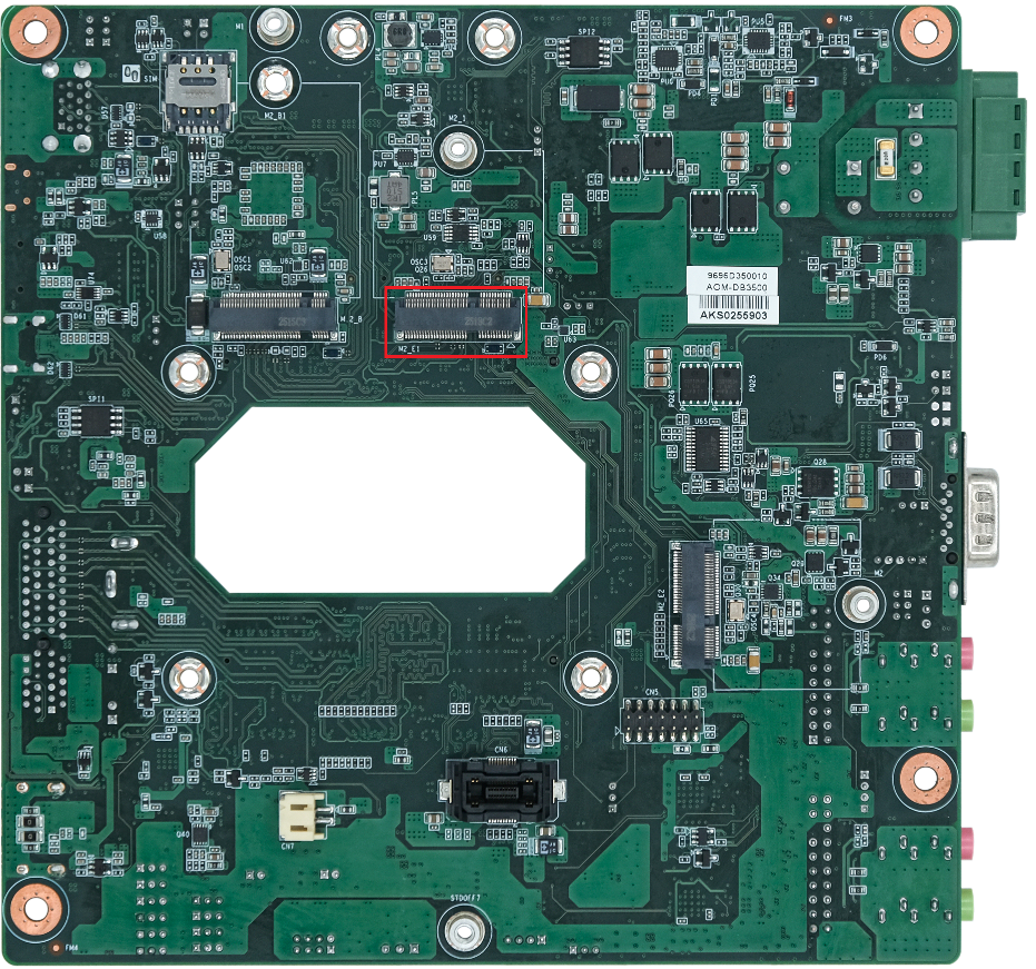
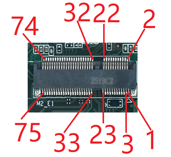
| − | [[File:AOM-DB3500 M2 E1.png]][[File:AOM-DB3500 M2 E1 Pin.png]] | + | [[File:AOM-DB3500 M2 E1.png|RTENOTITLE]][[File:AOM-DB3500 M2 E1 Pin.png|RTENOTITLE]] |
| + | |||
| + | === '''J8 M2_E1 Power Setting''' === | ||
| + | |||
| + | {| border="1" cellpadding="1" cellspacing="1" style="width: 500px;" | ||
| + | |- | ||
| + | | '''Pin''' | ||
| + | | '''Function''' | ||
| + | |- | ||
| + | | J8(1-2) | ||
| + | | M2_E1 power 3.3V (Default) | ||
| + | |- | ||
| + | | J8(2-3) | ||
| + | | M2_E1 power 3.8V | ||
| + | |} | ||
| + | |||
| + | === '''J9 M.2_B Power Setting''' === | ||
| + | |||
| + | {| border="1" cellpadding="1" cellspacing="1" style="width: 500px;" | ||
| + | |- | ||
| + | | style="width: 131px;" | '''Pin''' | ||
| + | | style="width: 355px;" | '''Function''' | ||
| + | |- | ||
| + | | style="width: 131px;" | J9(1-2) | ||
| + | | style="width: 355px;" | (B2B pin B76-B79) to M2_E1 (Default) | ||
| + | |- | ||
| + | | style="width: 131px;" | J9(2-3) | ||
| + | | style="width: 355px;" | UART1 (B2B pin B76-B79) to M2_E2 | ||
| + | |} | ||
| + | |||
| + | === '''WIFI/BT Support Modle:''' === | ||
| + | |||
| + | '''EWM-W179M201E RTL8852BE,Wifi6: PCIe + BT5.2: USB''' | ||
| + | |||
| + | '''AIW-162BS-GI1 Broadcom AP6275P, - 40°C~85°C PCIE+UART''' | ||
| + | |||
| + | === '''WIFI''' === | ||
| | ||
| + | |||
| + | === '''BT''' === | ||
Revision as of 09:32, 3 December 2025
Contents
M2_E1 Key Pin define
| M2_E1 M2_E1 Connector Pin Definition | |||
| Pin | Signal | I/O | Description |
| 1 | GND | Ground | |
| 2 | +V3.3E_M.2 | 3.3 V source | |
| 3 | USB5_Z_D+ | I/O | USB Data + Differential serial data |
| 4 | +V3.3E_M.2 | 3.3 V source | |
| 5 | USB5_Z_D- | I/O | USB Data - Differential serial data |
| 6 | LED1#_M2 | O | The Adapters’ status indicators via LED devices. |
| 7 | GND | Ground | |
| 8 | N/A | Not Applicable | |
| 9 | N/A | Not Applicable | |
| 10 | N/A | Not Applicable | |
| 11 | N/A | Not Applicable | |
| 12 | N/A | Not Applicable | |
| 13 | N/A | Not Applicable | |
| 14 | N/A | Not Applicable | |
| 15 | N/A | Not Applicable | |
| 16 | LED2#_M2 | O | The Adapters’ status indicators via LED devices. |
| 17 | N/A | Not Applicable | |
| 18 | GND | Ground | |
| 19 | N/A | Not Applicable | |
| 20 | UART1_E1_WAKE# | O | UART sideband used to Wake up Platform. |
| 21 | N/A | Not Applicable | |
| 22 | SER1_RX_M2 | O | UART Receive Data |
| 23 | N/A | Not Applicable | |
| 24-31 | Module key | Module key | |
| 32 | SER1_TX_M2 | I | UART Transmit Data |
| 33 | GND | Ground | |
| 34 | SER1_CTS#_M2 | O | UART Clear to Send connected. |
| 35 | PCIE20_A_TX+ | I | PCIe TX Differential signals. |
| 36 | SER1_RTS#_M2 | I | UART Ready to Send connected. |
| 37 | PCIE20_A_TX- | I | PCIe TX Differential signals |
| 38 | N/A | Not Applicable | |
| 39 | GND | Ground | |
| 40 | N/A | Not Applicable | |
| 41 | PCIE20_A_RX+ | O | PCIe RX Differential signals |
| 42 | N/A | Not Applicable | |
| 43 | PCIE20_A_RX- | O | PCIe RX Differential signals |
| 44 | N/A | Not Applicable | |
| 45 | GND | Ground | |
| 46 | N/A | Not Applicable | |
| 47 | PCIE20_A_CLK+ | I | PCIe Reference Clock signals (100 MHz) |
| 48 | N/A | Not Applicable | |
| 49 | PCIE20_A_CLK- | I | PCIe Reference Clock signals (100 MHz) |
| 50 | CLKO_Z_WIFI | I | Suspend Clock is a 32.768 kHz clock |
| 51 | GND | Ground | |
| 52 | PERST# | I | PCIe Reset is a functional reset to the Adapter |
| 53 | PCIE_Z_REQ# | I/O | PCIe Clock Request is a reference clock request signal. |
| 54 | NGFF_BT_DISABLE# | O | Aactive Low,when applied by the system it will disable radio operation on the Adapter that implement radio frequency applications. |
| 55 | PE_WAKE# | I/O | PCIe WAKE#. When the Adapter supports wakeup, this signal is used to request that the system return from asleep/suspend state to service a function wake initiated wake event. |
| 56 | NGFF_WIFI_DISABLE# | O | Aactive Low,when applied by the system it will disable radio operation on the Adapter that implement radio frequency applications. |
| 57 | GND | Ground | |
| 58 | EKEY_SDA | I/O | I2C data. |
| 59 | N/A | Not Applicable | |
| 60 | EKEY_SCL | I | I2C clock input from host. |
| 61 | N/A | Not Applicable | |
| 62 | EKEY1_ALERT# | O | Active Low.IRQ line to host processor. |
| 63 | GND | Ground | |
| 64 | N/A | Not Applicable | |
| 65 | N/A | Not Applicable | |
| 66 | N/A | Not Applicable | |
| 67 | N/A | Not Applicable | |
| 68 | N/A | Not Applicable | |
| 69 | GND | Ground | |
| 70 | N/A | Not Applicable | |
| 71 | N/A | Not Applicable | |
| 72 | +V3.3E_M.2 | 3.3 V source | |
| 73 | N/A | Not Applicable | |
| 74 | +V3.3E_M.2 | 3.3 V source | |
| 75 | EKEY_CARD_PRSNT# | I | The Signal is to control TS3A44159PWR and TS3A27518ERTWR output. |
J8 M2_E1 Power Setting
| Pin | Function |
| J8(1-2) | M2_E1 power 3.3V (Default) |
| J8(2-3) | M2_E1 power 3.8V |
J9 M.2_B Power Setting
| Pin | Function |
| J9(1-2) | (B2B pin B76-B79) to M2_E1 (Default) |
| J9(2-3) | UART1 (B2B pin B76-B79) to M2_E2 |
WIFI/BT Support Modle:
EWM-W179M201E RTL8852BE,Wifi6: PCIe + BT5.2: USB
AIW-162BS-GI1 Broadcom AP6275P, - 40°C~85°C PCIE+UART
WIFI

