Difference between revisions of "ROM-5880 user guide"
Xingxing.li (talk | contribs) |
Xingxing.li (talk | contribs) |
||
| (37 intermediate revisions by the same user not shown) | |||
| Line 1: | Line 1: | ||
| − | == ''' | + | |
| + | |||
| + | == '''产品特性(Features)''' == | ||
*Rockchip RK3568 Arm Quad Cortex-A55 up to 2.0GHz | *Rockchip RK3568 Arm Quad Cortex-A55 up to 2.0GHz | ||
*Onboard 2/4GB LPDDR4 memory and 16/32GB eMMC | *Onboard 2/4GB LPDDR4 memory and 16/32GB eMMC | ||
| − | *Support 1 x HDMI2.0 4K, 1 x signal LVDS or 1 x | + | *Support 1 x HDMI2.0 4K, 1 x signal LVDS or 1 x MIPI DSI |
*Support 4K H.264/H.265 Video decoder | *Support 4K H.264/H.265 Video decoder | ||
*2 x USB3.0, 2 x USB2.0, 4 x UART, 14 x GPIO | *2 x USB3.0, 2 x USB2.0, 4 x UART, 14 x GPIO | ||
| Line 10: | Line 12: | ||
*Support Linux & Android | *Support Linux & Android | ||
| − | == ''' | + | === '''产品官网链接(Product official website link)''' === |
| − | |||
| − | |||
| − | + | [https://www.advantech.com.cn/zh-cn/products/77b59009-31a9-4751-bee1-45827a844421/rom-5880/mod_e0d210fc-532a-4075-896f-0b80c13380fc ROM-5880 - 基于瑞芯微RK3568平台的SMARC2.1核心模块 - 研华 (advantech.com.cn)] | |
| − | + | == '''接口布局和尺寸(Layout and Sizes)''' == | |
| − | == ''' | + | === '''ROM-5880接口布局图 Board Dimension Layout''' === |
| − | |||
| − | |||
| − | |||
| − | |||
| − | |||
| − | |||
| − | |||
| − | |||
[[File:ROM-5880 Connector Location.png|RTENOTITLE]] | [[File:ROM-5880 Connector Location.png|RTENOTITLE]] | ||
| Line 70: | Line 62: | ||
[[File:ROM-5880 AT ATX mode.png|RTENOTITLE]] | [[File:ROM-5880 AT ATX mode.png|RTENOTITLE]] | ||
| − | == '''SOM-DB2510 A1 Board Dimension Layout''' == | + | === '''SOM-DB2510 A1 Board Dimension Layout''' === |
The figures below indicate the main chips on SOM-DB2510 Development Board for SMARC 2.1. | The figures below indicate the main chips on SOM-DB2510 Development Board for SMARC 2.1. | ||
| Line 83: | Line 75: | ||
[[File:SOM-DB2510 Connect Locations 1.png|RTENOTITLE]] | [[File:SOM-DB2510 Connect Locations 1.png|RTENOTITLE]] | ||
| − | |||
| − | |||
| − | |||
| − | |||
| − | |||
| − | |||
'''Switch Locations''' | '''Switch Locations''' | ||
| Line 106: | Line 92: | ||
[[File:SOM-DB2510 LED Locations.png|RTENOTITLE]] | [[File:SOM-DB2510 LED Locations.png|RTENOTITLE]] | ||
| − | + | {| border="1" cellpadding="1" cellspacing="1" | |
| + | |- | ||
| + | | '''Label''' | ||
| + | | '''Function''' | ||
| + | | '''Label''' | ||
| + | | '''Function''' | ||
| + | |- | ||
| + | | ATX1 | ||
| + | | ATX Connector | ||
| + | | FAN1 | ||
| + | | Smart Fan Connector | ||
| + | |- | ||
| + | | SMARC_IN1 | ||
| + | | Wide Range Input Power Connector (3V~5.25V) | ||
| + | | FAN2 | ||
| + | | System Fan Connector | ||
| + | |- | ||
| + | | DCIN1 | ||
| + | | DCIN connector | ||
| + | | CAN0_1 | ||
| + | | CAN Bus Connector | ||
| + | |- | ||
| + | | DP0_HDMI | ||
| + | | DP & HDMI Connector | ||
| + | | USB0 | ||
| + | | USB OTG Connector | ||
| + | |- | ||
| + | | USB12 | ||
| + | | USB 2.0 port1~2 & USB 3.0 port0 Connector | ||
| + | | COM1_3 | ||
| + | | COM Port Port1,3 Connector | ||
| + | |- | ||
| + | | TYPEC_DP1 | ||
| + | | Type-C Connector | ||
| + | | COM2_4 | ||
| + | | COM Port Port2,4 Connector | ||
| + | |- | ||
| + | | LAN0_LAN1 | ||
| + | | LAN0 & LAN1 Connector | ||
| + | | CN8 | ||
| + | | I2C connector for I2C_PM | ||
| + | |- | ||
| + | | LOUT1 | ||
| + | | Line Out Connector | ||
| + | | CN7 | ||
| + | | I2C Connector for I2C_GP | ||
| + | |- | ||
| + | | MIC1 | ||
| + | | MIC1 Connector | ||
| + | | CN10 | ||
| + | | eSPI Pin Header | ||
| + | |- | ||
| + | | CN1_MXM1 | ||
| + | | SMARC Connector | ||
| + | | SATAP1 | ||
| + | | SATA Power Connector | ||
| + | |- | ||
| + | | PCIEA-X4 | ||
| + | | PCIe x4 Connector | ||
| + | | CSI0_B2B | ||
| + | | MIPI B2B Connector for 2M Camera | ||
| + | |- | ||
| + | | SATA1 | ||
| + | | SATA Port0 Connector | ||
| + | | CSI1_B2B | ||
| + | | MIPI B2B Connector for 8M & 13M Camera | ||
| + | |- | ||
| + | | PCIED-X1 | ||
| + | | PCIe x1 Connector | ||
| + | | SPI_BIOS1 | ||
| + | | Carrier Board BIOS Socket (SOIC) | ||
| + | |- | ||
| + | | M2 | ||
| + | | M.2 Key-E Connector | ||
| + | | BAT1 | ||
| + | | Coin battery holder | ||
| + | |- | ||
| + | | MPCIE_C | ||
| + | | Mini PCIe Connector | ||
| + | | BAT2 | ||
| + | | Smart battery Connector | ||
| + | |- | ||
| + | | SIM | ||
| + | | SIM card Connector | ||
| + | | LINEOUT_1 | ||
| + | | I2S Headphone Connector | ||
| + | |- | ||
| + | | LVDS1 | ||
| + | | LVDS1 Connector | ||
| + | | MIC_1 | ||
| + | | I2S MIC In Connector | ||
| + | |- | ||
| + | | LVDS0 | ||
| + | | LVDS0 Connector | ||
| + | | CSI1_FPC | ||
| + | | MIPI FPC Connector for 8M & 13M Camera | ||
| + | |- | ||
| + | | LVDS1_INVERTER | ||
| + | | LVDS1 Invertor Connector | ||
| + | | CSI0_FPC | ||
| + | | MIPI FPC Connector for 2M Camera | ||
| + | |- | ||
| + | | LVDS0_INVERTER | ||
| + | | LVDS0 Invertor Connector | ||
| + | | CN5 | ||
| + | | I2S2 Connector | ||
| + | |- | ||
| + | | SPI_BIOS2 | ||
| + | | Carrier Board BIOS Socket (QFN) | ||
| + | | CN17 | ||
| + | | I2S0 Connector | ||
| + | |- | ||
| + | | SD | ||
| + | | SD Card Connector | ||
| + | | | ||
| + | | | ||
| + | |} | ||
| − | + | '''Jumper Locations''' | |
| − | [[Jumper | + | [[File:SOM DB2510 Jumper Locations.png|RTENOTITLE]] |
| − | [[ | + | [[File:SOM-DB2510 Jumper Locations1.png|RTENOTITLE]] |
| − | + | {| border="1" cellpadding="1" cellspacing="1" | |
| + | |- | ||
| + | | Lable | ||
| + | | Function | ||
| + | | Lable | ||
| + | | Function | ||
| + | |- | ||
| + | | BTN3 | ||
| + | | Sleep Button | ||
| + | | J14 | ||
| + | | EDP1/LVDS1 Hot-Plug Detect Selection Header | ||
| + | |- | ||
| + | | BTN1 | ||
| + | | Power Button | ||
| + | | J56 | ||
| + | | Standby Voltage Control Header | ||
| + | |- | ||
| + | | BTN2 | ||
| + | | Reset Button | ||
| + | | J44 | ||
| + | | Module +3.3V/+5V Power Selection Header | ||
| + | |- | ||
| + | | SW4 | ||
| + | | BOOT SELECT Switch | ||
| + | | PSON1 | ||
| + | | AT/ATX Selection Header | ||
| + | |- | ||
| + | | LID1 | ||
| + | | LID Switch | ||
| + | | SPI_CN1 | ||
| + | | SPI Header | ||
| + | |- | ||
| + | | J30 | ||
| + | | Enable Battery Low# Header | ||
| + | | CN14 | ||
| + | | For CAN Bus port0 Terminal Resistor | ||
| + | |- | ||
| + | | M2E_DISABLE_N1 | ||
| + | | M.2 Wireless Disable | ||
| + | | CN15 | ||
| + | | For CAN Bus port1 Terminal Resistor | ||
| + | |- | ||
| + | | J29 | ||
| + | | SMB Alert Enable Header | ||
| + | | J3/J4 | ||
| + | | DP0 EQ0 Selection | ||
| + | |- | ||
| + | | CN9 | ||
| + | | Header For GPIO Test | ||
| + | | J5/J6 | ||
| + | | DP0 EQ1 Selection | ||
| + | |- | ||
| + | | J7/J8 | ||
| + | | LVDS0 Power Selection Header | ||
| + | | J58 | ||
| + | | PCIE_B_CKREQ# Selection | ||
| + | |- | ||
| + | | J11/J12 | ||
| + | | LVDS1 Power Selection Header | ||
| + | | J59 | ||
| + | | PCIE_A_CKREQ# Selection | ||
| + | |- | ||
| + | | J9 | ||
| + | | LVDS0 Inverter Power Selection Heade | ||
| + | | GPIO_0 | ||
| + | | GPIO0/CAM0_PWR# Selection | ||
| + | |- | ||
| + | | J10 | ||
| + | | EDP0/LVDS0 Hot-Plug Detect Selection Header | ||
| + | | GPIO_1 | ||
| + | | GPIO1/CAM1_PWR# Selection | ||
| + | |- | ||
| + | | J26 | ||
| + | | HDA/I2S Selection Header | ||
| + | | GPIO_2 | ||
| + | | GPIO2/CAM0_RST# Selection | ||
| + | |- | ||
| + | | J1 | ||
| + | | DP1/HDMI1 Select | ||
| + | | GPIO_3 | ||
| + | | GPIO3/CAM1_RST# Selection | ||
| + | |- | ||
| + | | J13 | ||
| + | | LVDS1 Inverter Power Selection Header | ||
| + | | GPIO_4 | ||
| + | | GPIO4/HDA_RST# Selection | ||
| + | |- | ||
| + | | J31 | ||
| + | | Clear CMOS Header | ||
| + | | GPIO_5 | ||
| + | | GPIO5/PWM_OUT Selection | ||
| + | |- | ||
| + | | J25 | ||
| + | | SPI Power Header | ||
| + | | GPIO_6 | ||
| + | | GPIO6/TACHIN Selection | ||
| + | |- | ||
| + | | SW1 | ||
| + | | COM1 mode Select | ||
| + | | SATA_ACT_PH1 | ||
| + | | SATA act# Header | ||
| + | |- | ||
| + | | SW2 | ||
| + | | COM3 mode Select | ||
| + | | PWRBTN_PH1 | ||
| + | | Power button Header | ||
| + | |- | ||
| + | | J41 | ||
| + | | Core Power Voltage Control Header | ||
| + | | SYS_RESET_PH1 | ||
| + | | Reset button Header | ||
| + | |- | ||
| + | | J2 | ||
| + | | DDI1 AUX/DDC Selection | ||
| + | | | ||
| + | | | ||
| + | |} | ||
| − | + | === '''LED Function List ''' === | |
| − | + | {| border="1" cellpadding="1" cellspacing="1" | |
| + | |- | ||
| + | | Location | ||
| + | | Function | ||
| + | |- | ||
| + | | MODULE_VIN_LED1 | ||
| + | | WDT_TIME_OUT# Indicate | ||
| + | |- | ||
| + | | MODULE_5V_LED | ||
| + | | Module 5V Indicate | ||
| + | |- | ||
| + | | MODULE_VIN_LED | ||
| + | | Module +V_MOD_IN Indicate | ||
| + | |- | ||
| + | | RESET_OUT_LED | ||
| + | | RESET_OUT Indicate | ||
| + | |- | ||
| + | | RESET_OUT_LED | ||
| + | | CARRIER_STBY Indicate | ||
| + | |- | ||
| + | | CARRIER_PWR_ON_LED | ||
| + | | CARRIER_PWR_ON Indicate | ||
| + | |- | ||
| + | | MODULE_3P3V_LED | ||
| + | | Module 3.3V Indicate | ||
| + | |- | ||
| + | | 3P3V_LED | ||
| + | | Carrier Board +V3.3 Indicate | ||
| + | |- | ||
| + | | 5V_LED | ||
| + | | Carrier Board +V5 Indicate | ||
| + | |- | ||
| + | | 5V_DUAL_LED | ||
| + | | Carrier Board +V5SB Indicate | ||
| + | |- | ||
| + | | 3P3V_DUAL_LED | ||
| + | | Carrier Board +V3.3SB Indicate | ||
| + | |- | ||
| + | | 5VA_LED | ||
| + | | Carrier Board +V5D_MOD Indicate | ||
| + | |- | ||
| + | | SATA_LED | ||
| + | | SATA Indicate | ||
| + | |- | ||
| + | | SOM_LED | ||
| + | | SOM BOM Indicate | ||
| + | |- | ||
| + | | RISC_LED | ||
| + | | RISC BOM Indicate | ||
| + | |} | ||
| − | == '''ROM-5880 机械尺寸(Mechanical Characteristics)''' == | + | === '''Switch Settings''' === |
| + | |||
| + | *[[SW4|SW4]] (Boot Select/Force Recovery/Test Switches) | ||
| + | *[[LID1|LID1]] (LID Button Enable/Disable Switches) | ||
| + | *[[SW5|SW5 ]](LAN CONN LED Pull High Switches) | ||
| + | *[[COM0_Settings|SW1]](COM0 Settings) | ||
| + | *[[SW2|SW2]](COM2 Settings) | ||
| + | *[[I2S_Clock_Settings|SW3 ]](I2S Clock Settings) | ||
| + | *[[M2E_DISABLE_N1|M2E_DISABLE_N1]](M.2 Wireless Disable Switch) | ||
| + | |||
| + | === '''接口引脚定義 (Connector Pin definitions)''' === | ||
| + | |||
| + | *[[ATX1_Pin_Connector| ATX1 Pin Connector]] | ||
| + | *[[SMARC_IN1_Pin_Connectors|SMARC_IN1 Pin Connectors]] | ||
| + | *[[BAT1_RTC_Battery_Connectors|BAT1 RTC Battery Connectors]] | ||
| + | *[[DCIN1_DC-IN_Power_Connectors|DCIN1 DC-IN Power Connectors]] | ||
| + | *[[CAN0_1_CAN_Bus_Connectors|CAN0_1 CAN Bus Connectors]] | ||
| + | *[[CN9_GPIO_Headers|CN9 GPIO Headers]] | ||
| + | *[[COM2_4_COM_Port2&4_Connectors|COM2_4 COM Port2&4 Connectors]] | ||
| + | *[[COM1_3_COM_Port1&_3_Connectors|COM1_3 COM Port1& 3 Connectors]] | ||
| + | *[[CN10_ESPI_Headers|CN10 ESPI Headers]] | ||
| + | *[[LVDS0_LVDS_Connectors|LVDS0 LVDS Connectors]] | ||
| + | *[[LVDS0_INVERTER_LVDS_INVERTER_Connectors|LVDS0_INVERTER LVDS INVERTER Connectors]] | ||
| + | *[[LVDS1_LVDS_Connectors|LVDS1 LVDS Connectors]] | ||
| + | *[[LVDS1_INVERTER_LVDS_INVERTER_Connectors|LVDS1_INVERTER LVDS INVERTER Connectors]] | ||
| + | *[[CN7_I2C_GP_Connectors|CN7 I2C_GP Connectors]] | ||
| + | *[[SPI_CN1_SPI_Connectors|SPI_CN1 SPI Connectors]] | ||
| + | *[[SATAP1_SATA_PWR_Connectors|SATAP1 SATA PWR Connectors]] | ||
| + | *[[CSI0_FPC_Connectors|CSI0_FPC Connectors]] | ||
| + | *[[CSI1_FPC_Connectors|CSI1_FPC Connectors]] | ||
| + | *[[CN5_I2S2_Connectors|CN5 I2S2 Connectors]] | ||
| + | *[[CN17_I2S0_Connectors|CN17 I2S0 Connectors]] | ||
| + | *[[PWRBTN_PH1_PWRBTN_Pin_Headers|PWRBTN_PH1 PWRBTN Pin Headers]] | ||
| + | *[[SYS_RESET_PH1_SYS_RESET_Pin_Headers|SYS_RESET_PH1 SYS RESET Pin Headers]] | ||
| + | *[[SATA_ACT_PH1_SATA_ACT|SATA_ACT_PH1 SATA ACT# Pin Headers]] | ||
| + | *[[J32_Power_LED_Pin_Headers|J32 Power LED Pin Headers]] | ||
| + | *[[J30_BATLOW_Pin_Headers|J30 BATLOW Pin Headers]] | ||
| + | *[[J29_SMBUS_Alert_Pin_Headers|J29 SMBUS Alert Pin Headers]] | ||
| + | *[[J41_Core_Power_Controls|J41 Core Power Controls]] | ||
| + | *[[PSON1_ATX/AT_Mode_Selection|PSON1 ATX/AT Mode Selection]] | ||
| + | *[[J56_Standby_Power_Controls|J56 Standby Power Controls]] | ||
| + | *[[J44_Module_Power_Settings|J44 Module Power Settings]] | ||
| + | *[[J7,J8_LVDS0_Power_Selection|J7,J8 LVDS0 Power Selection]] | ||
| + | *[[J9_LVDS0_Inverter_Power_Selection|J9 LVDS0 Inverter Power Selection]] | ||
| + | *[[J11,J12_LVDS1_Power_Selection|J11,J12 LVDS1 Power Selection]] | ||
| + | *[[LVDS1_Inverter_Power_Selection|LVDS1 Inverter Power Selection]] | ||
| + | *[[EDP0_/LVDS0_HPD_Selection|EDP0 /LVDS0 HPD Selection]] | ||
| + | *[[J14_EDP1/LVDS1_HPD_Selection|J14 EDP1/LVDS1 HPD Selection]] | ||
| + | *[[CN14_CAN0_Terminal_Resistor_Selection|CN14 CAN0 Terminal Resistor Selection]] | ||
| + | *[[CN15_CAN1_Terminal_Resistor_Selection|CN15 CAN1 Terminal Resistor Selection]] | ||
| + | *[[J2_DDI1_AUX/DDC_Selection|J2 DDI1 AUX/DDC Selection]] | ||
| + | *[[J1_DP1/HDMI1_Selection|J1 DP1/HDMI1 Selection]] | ||
| + | *[[J58_PCIE_B_CKREQ|J58 PCIE_B_CKREQ# Selection]] | ||
| + | *[[J59_PCIE_A_CKREQ|J59 PCIE_A_CKREQ# Selection]] | ||
| + | *[[J31_Clear_CMOS|J31 Clear CMOS]] | ||
| + | *[[J25_+V1.8M_SPI_Power_Jumpers|J25 +V1.8M_SPI Power Jumpers]] | ||
| + | *[[GPIO_0_GPIO0_Settings|GPIO_0 GPIO0 Settings]] | ||
| + | *[[GPIO_1_GPIO1_Settings|GPIO_1 GPIO1 Settings]] | ||
| + | *[[GPIO_2_GPIO2_Settings|GPIO_2 GPIO2 Settings]] | ||
| + | *[[GPIO_3_GPIO3_Settings|GPIO_3 GPIO3 Settings]] | ||
| + | *[[GPIO_4_GPIO4_Settings|GPIO_4 GPIO4 Settings]] | ||
| + | *[[GPIO_5_GPIO5_Settings|GPIO_5 GPIO5 Settings]] | ||
| + | *[[GPIO_6_GPIO6_Settings|GPIO_6 GPIO6 Settings]] | ||
| + | *[[J26_HDA/I2S_Selection|J26 HDA/I2S Selection]] | ||
| + | |||
| + | === '''ROM-5880 机械尺寸(Mechanical Characteristics)''' === | ||
*'''Dimension: SMARC form factor size: (D x W) 82 x 50 mm/3.22 x 1.9 in''' | *'''Dimension: SMARC form factor size: (D x W) 82 x 50 mm/3.22 x 1.9 in''' | ||
| + | |||
| + | [[File:ROM-5880 Dimensions.png|RTENOTITLE]] | ||
| + | |||
*'''Height on top: Under 3.0 mm''' | *'''Height on top: Under 3.0 mm''' | ||
*'''Height on bottom: Under 2.0 mm''' | *'''Height on bottom: Under 2.0 mm''' | ||
| Line 128: | Line 463: | ||
[[File:ROM-5880 Mechanical Specifications.png|RTENOTITLE]] | [[File:ROM-5880 Mechanical Specifications.png|RTENOTITLE]] | ||
| − | + | === '''SOM-DB2510_A1 机械尺寸 ('''Mechanical Characteristics) === | |
| − | == '''SOM-DB2510_A1 机械尺寸 ('''Mechanical Characteristics) == | ||
For more details regarding our 2D/3D models, please visit the Advantech COM support service website at: [http://com.advantech.com http://com.advantech.com]. | For more details regarding our 2D/3D models, please visit the Advantech COM support service website at: [http://com.advantech.com http://com.advantech.com]. | ||
| Line 135: | Line 469: | ||
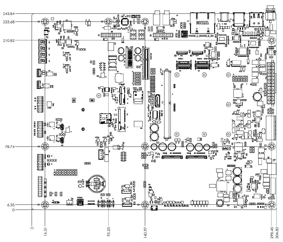
=== '''Board Mechanical Diagram -Front''' === | === '''Board Mechanical Diagram -Front''' === | ||
| − | [[File:SOM-DB2510 Board Mechanical Diagram - Front.png]] | + | [[File:SOM-DB2510 Board Mechanical Diagram - Front.png|RTENOTITLE]] |
'''Board Mechanical Diagram -Side1''' | '''Board Mechanical Diagram -Side1''' | ||
| Line 145: | Line 479: | ||
[[File:SOM-DB2510 Board Mechanical Diagram Side2.png|RTENOTITLE]] | [[File:SOM-DB2510 Board Mechanical Diagram Side2.png|RTENOTITLE]] | ||
| + | | ||
=== '''Assemblly Diagram''' === | === '''Assemblly Diagram''' === | ||
| Line 150: | Line 485: | ||
These figures demonstrate the order of assembly needed when attaching the thermal module and COM module to the carrier board. | These figures demonstrate the order of assembly needed when attaching the thermal module and COM module to the carrier board. | ||
| − | [[File:ROM-5880 for SOM-DB2510 Assembly Diagram.png]] | + | [[File:ROM-5880 for SOM-DB2510 Assembly Diagram.png|RTENOTITLE]] |
| + | |||
== '''快速入门 (Quick Start)''' == | == '''快速入门 (Quick Start)''' == | ||
| − | |||
| − | |||
| − | |||
| − | |||
=== '''系统下载 (OS Download)''' === | === '''系统下载 (OS Download)''' === | ||
| + | <div>Note:LIV=Yocto Linux , UIV=Ubuntu,DIV=Debain,AIV=Android </div> | ||
| + | LBV=BSP,LIV=Image | ||
| − | + | {| border="1" cellpadding="1" cellspacing="1" | |
| − | |||
| − | |||
| − | |||
| − | |||
| − | |||
| − | {| border="1" cellpadding="1" cellspacing="1 | ||
|- | |- | ||
| − | + | | '''Platform''' | |
| − | + | | '''Product''' | |
| − | + | | '''Image Version''' | |
| − | + | | '''Release Date''' | |
| − | + | | '''Release Version''' | |
| − | + | | '''Release notes''' | |
| − | + | | '''Image Download''' | |
| − | + | | '''BSP Download Tag''' | |
| − | | | + | | '''Comment''' |
| + | | '''CAN2.0 Patch''' | ||
|- | |- | ||
| − | + | | RK3568 | |
| − | + | | ROM-5880 | |
| − | | | + | | DIV130033 |
| − | + | | 2023/08/29 | |
| − | | | + | | RTM |
| − | + | | [http://ess-wiki.advantech.com.tw/view/AIM-Linux/BSP/RockChip/Linux_Debian_OS_Release_note/ROM-5880/DIV130033 Release_Note] | |
| − | + | | | |
| − | [https://pan.baidu.com/s/ | + | [https://pan.baidu.com/s/1oJb5kMPtSyvsNxmmuebm5A Baidu] Password:a887 |
| − | [https://www.dropbox.com/ | + | [https://www.dropbox.com/sh/a8tjyodf4a3mxpb/AAAsLlKReCHtnyZzyP-hNOhFa?dl=0 Dropbox] |
| − | | | + | | RK3568_RISC_DIV130033.xml |
| − | + | | | |
| − | + | '''[https://pan.baidu.com/s/1WeQwXmE409gA4vJxhRqusg?pwd=a887 CAN2.0 Errata ] ''' | |
| − | |||
| − | |||
| − | |||
| − | |||
| − | |||
| − | |||
| − | |||
| − | [https://pan.baidu.com/s/ | ||
| − | + | 提取码:a887 | |
| − | | | + | | [https://pan.baidu.com/s/1I5MOuiH3uVn2xJjP8VuVVA?pwd=a887 Baidu] Password:a887 |
| − | |||
|} | |} | ||
| Line 213: | Line 533: | ||
*GA: Beta version by QE verification; | *GA: Beta version by QE verification; | ||
| − | *RTM: Beta version by SI/Power/QE verification and pre-loaded; | + | *RTM: Beta version by SI/Power/QE verification and pre-loaded; |
| + | |||
| + | === '''Debian 燒錄方法 (Debiand Flash eMMC Method)''' === | ||
| + | |||
| + | <span style="color:#2980b9;">'''1.''' </span>[[1.Usering_RKTool.|<span style="color:#2980b9;">'''Usering_RKTool.'''</span>]] | ||
| + | '''<span style="color:#2980b9;">2. </span>[[Using_bootup_sd_disk_made_by_SDDiskTool_for_ROM-5880|<span style="color:#2980b9;">Usering bootup_sd_disk made_by SDDiskTool.</span>]]''' | ||
| − | + | '''<span style="color:#2980b9;">3. [[Upgrade_with_system_command_for_ROM-5880|Upgrade with system command.]]</span>''' | |
| − | == | + | == '''Linux基本使用方法''' == |
| − | + | *[[Getting_Start(ROM-5880)|'''Getting Start''']] | |
| + | *'''[[ROM-5880_QT_ToolsChain|QT_ToolsChain]]''' | ||
| + | *[[ROM-5880_NPU_SDK|'''NPU_SDK''']] | ||
| + | *'''MAC_Address''' | ||
| − | == ''' | + | == '''Linux BSP编译方法(Linux BSP Compile Method)''' == |
| − | + | [[Linux_BSP_User_Guide_for_rk3568-ROM5880_series_Debain_10|'''Linux_BSP_User_Guide_for_rk3568_series_Debain_10''']] | |
Latest revision as of 06:40, 24 June 2024
Contents
- 1 产品特性(Features)
- 2 接口布局和尺寸(Layout and Sizes)
- 2.1 ROM-5880接口布局图 Board Dimension Layout
- 2.2 Connector List
- 2.3 SOM-DB2510 A1 Board Dimension Layout
- 2.4 SOM-DB2510 Connectors and Jumper Settings
- 2.5 LED Function List
- 2.6 Switch Settings
- 2.7 接口引脚定義 (Connector Pin definitions)
- 2.8 ROM-5880 机械尺寸(Mechanical Characteristics)
- 2.9 SOM-DB2510_A1 机械尺寸 (Mechanical Characteristics)
- 2.10 Board Mechanical Diagram -Front
- 2.11 Assemblly Diagram
- 3 快速入门 (Quick Start)
- 4 Linux基本使用方法
- 5 Linux BSP编译方法(Linux BSP Compile Method)
产品特性(Features)
- Rockchip RK3568 Arm Quad Cortex-A55 up to 2.0GHz
- Onboard 2/4GB LPDDR4 memory and 16/32GB eMMC
- Support 1 x HDMI2.0 4K, 1 x signal LVDS or 1 x MIPI DSI
- Support 4K H.264/H.265 Video decoder
- 2 x USB3.0, 2 x USB2.0, 4 x UART, 14 x GPIO
- 2 x PCIe3.0, 1 x SATA, 1 x MIPI CSI, 2 x Gigabit LAN
- Support Linux & Android
产品官网链接(Product official website link)
ROM-5880 - 基于瑞芯微RK3568平台的SMARC2.1核心模块 - 研华 (advantech.com.cn)
接口布局和尺寸(Layout and Sizes)
ROM-5880接口布局图 Board Dimension Layout
Connector List
Debug
| Position | Description |
| DEBUG | DEBUG Port |
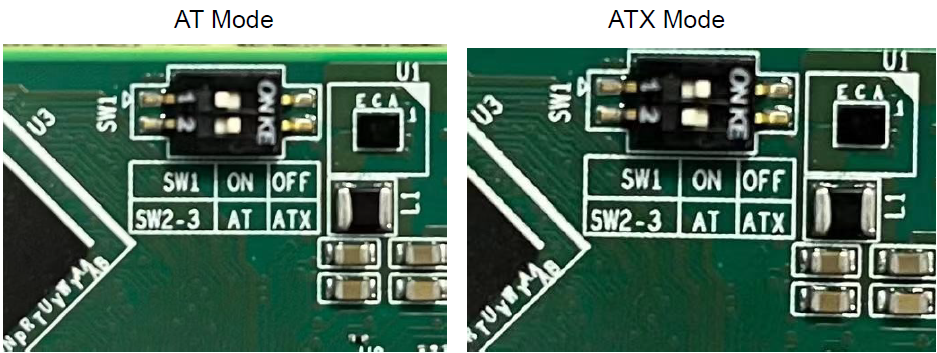
Switch
| Position | Description |
| SW1 | AT&ATX mode selection |
SW1:AT/ATX Mode Selection
| Setting | Function |
| 1 off 2 on | AT Mode(Default) |
| 1 on 2 off | ATX Mode |
SOM-DB2510 A1 Board Dimension Layout
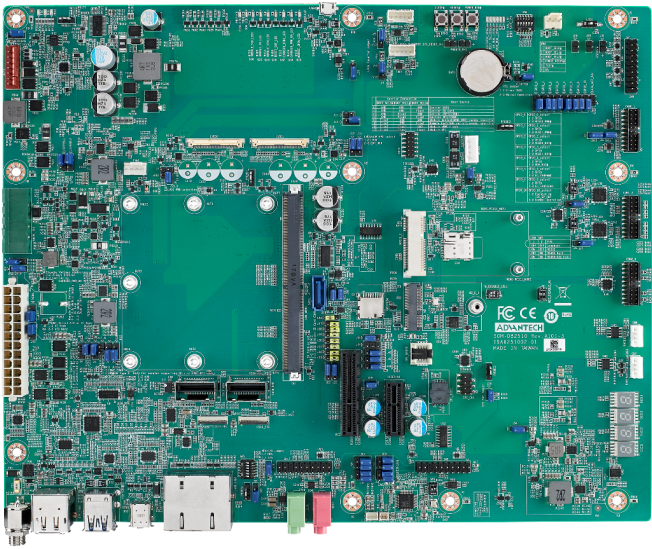
The figures below indicate the main chips on SOM-DB2510 Development Board for SMARC 2.1.
SOM-DB2510 Connectors and Jumper Settings
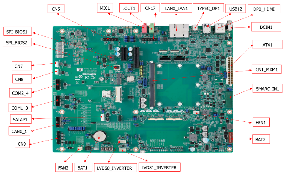
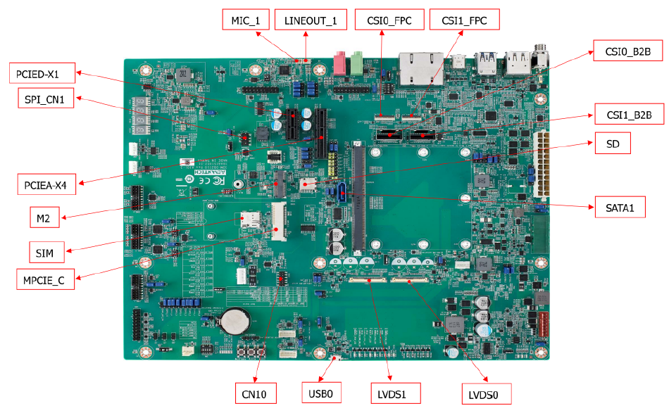
Connector Locations
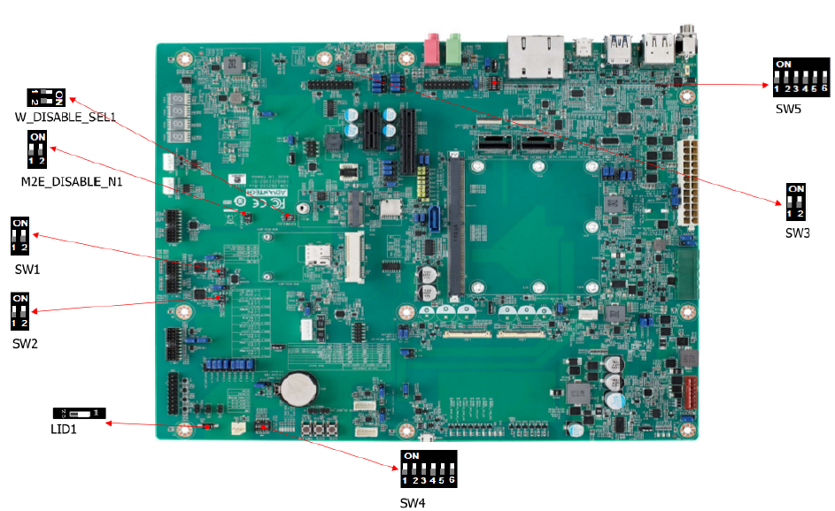
Switch Locations
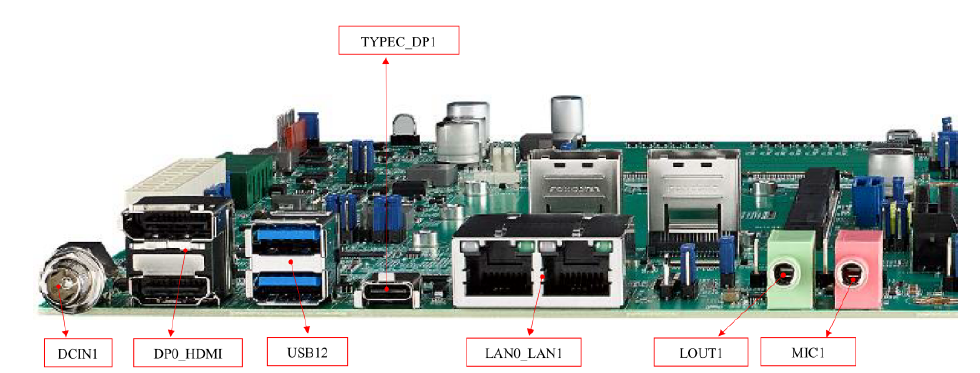
I/O Connctor Locations
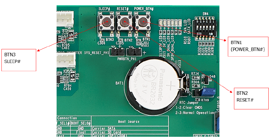
Button Locations
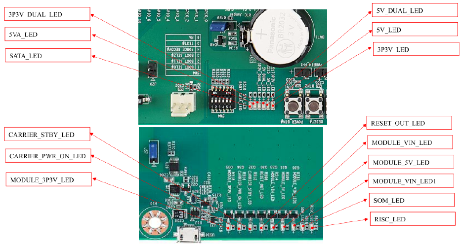
LED Locations
| Label | Function | Label | Function |
| ATX1 | ATX Connector | FAN1 | Smart Fan Connector |
| SMARC_IN1 | Wide Range Input Power Connector (3V~5.25V) | FAN2 | System Fan Connector |
| DCIN1 | DCIN connector | CAN0_1 | CAN Bus Connector |
| DP0_HDMI | DP & HDMI Connector | USB0 | USB OTG Connector |
| USB12 | USB 2.0 port1~2 & USB 3.0 port0 Connector | COM1_3 | COM Port Port1,3 Connector |
| TYPEC_DP1 | Type-C Connector | COM2_4 | COM Port Port2,4 Connector |
| LAN0_LAN1 | LAN0 & LAN1 Connector | CN8 | I2C connector for I2C_PM |
| LOUT1 | Line Out Connector | CN7 | I2C Connector for I2C_GP |
| MIC1 | MIC1 Connector | CN10 | eSPI Pin Header |
| CN1_MXM1 | SMARC Connector | SATAP1 | SATA Power Connector |
| PCIEA-X4 | PCIe x4 Connector | CSI0_B2B | MIPI B2B Connector for 2M Camera |
| SATA1 | SATA Port0 Connector | CSI1_B2B | MIPI B2B Connector for 8M & 13M Camera |
| PCIED-X1 | PCIe x1 Connector | SPI_BIOS1 | Carrier Board BIOS Socket (SOIC) |
| M2 | M.2 Key-E Connector | BAT1 | Coin battery holder |
| MPCIE_C | Mini PCIe Connector | BAT2 | Smart battery Connector |
| SIM | SIM card Connector | LINEOUT_1 | I2S Headphone Connector |
| LVDS1 | LVDS1 Connector | MIC_1 | I2S MIC In Connector |
| LVDS0 | LVDS0 Connector | CSI1_FPC | MIPI FPC Connector for 8M & 13M Camera |
| LVDS1_INVERTER | LVDS1 Invertor Connector | CSI0_FPC | MIPI FPC Connector for 2M Camera |
| LVDS0_INVERTER | LVDS0 Invertor Connector | CN5 | I2S2 Connector |
| SPI_BIOS2 | Carrier Board BIOS Socket (QFN) | CN17 | I2S0 Connector |
| SD | SD Card Connector |
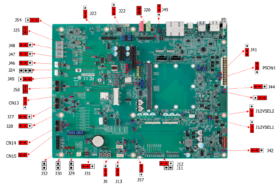
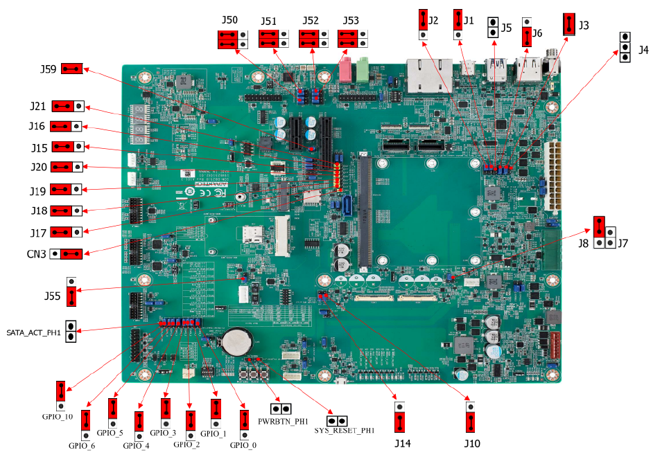
Jumper Locations
| Lable | Function | Lable | Function |
| BTN3 | Sleep Button | J14 | EDP1/LVDS1 Hot-Plug Detect Selection Header |
| BTN1 | Power Button | J56 | Standby Voltage Control Header |
| BTN2 | Reset Button | J44 | Module +3.3V/+5V Power Selection Header |
| SW4 | BOOT SELECT Switch | PSON1 | AT/ATX Selection Header |
| LID1 | LID Switch | SPI_CN1 | SPI Header |
| J30 | Enable Battery Low# Header | CN14 | For CAN Bus port0 Terminal Resistor |
| M2E_DISABLE_N1 | M.2 Wireless Disable | CN15 | For CAN Bus port1 Terminal Resistor |
| J29 | SMB Alert Enable Header | J3/J4 | DP0 EQ0 Selection |
| CN9 | Header For GPIO Test | J5/J6 | DP0 EQ1 Selection |
| J7/J8 | LVDS0 Power Selection Header | J58 | PCIE_B_CKREQ# Selection |
| J11/J12 | LVDS1 Power Selection Header | J59 | PCIE_A_CKREQ# Selection |
| J9 | LVDS0 Inverter Power Selection Heade | GPIO_0 | GPIO0/CAM0_PWR# Selection |
| J10 | EDP0/LVDS0 Hot-Plug Detect Selection Header | GPIO_1 | GPIO1/CAM1_PWR# Selection |
| J26 | HDA/I2S Selection Header | GPIO_2 | GPIO2/CAM0_RST# Selection |
| J1 | DP1/HDMI1 Select | GPIO_3 | GPIO3/CAM1_RST# Selection |
| J13 | LVDS1 Inverter Power Selection Header | GPIO_4 | GPIO4/HDA_RST# Selection |
| J31 | Clear CMOS Header | GPIO_5 | GPIO5/PWM_OUT Selection |
| J25 | SPI Power Header | GPIO_6 | GPIO6/TACHIN Selection |
| SW1 | COM1 mode Select | SATA_ACT_PH1 | SATA act# Header |
| SW2 | COM3 mode Select | PWRBTN_PH1 | Power button Header |
| J41 | Core Power Voltage Control Header | SYS_RESET_PH1 | Reset button Header |
| J2 | DDI1 AUX/DDC Selection |
LED Function List
| Location | Function |
| MODULE_VIN_LED1 | WDT_TIME_OUT# Indicate |
| MODULE_5V_LED | Module 5V Indicate |
| MODULE_VIN_LED | Module +V_MOD_IN Indicate |
| RESET_OUT_LED | RESET_OUT Indicate |
| RESET_OUT_LED | CARRIER_STBY Indicate |
| CARRIER_PWR_ON_LED | CARRIER_PWR_ON Indicate |
| MODULE_3P3V_LED | Module 3.3V Indicate |
| 3P3V_LED | Carrier Board +V3.3 Indicate |
| 5V_LED | Carrier Board +V5 Indicate |
| 5V_DUAL_LED | Carrier Board +V5SB Indicate |
| 3P3V_DUAL_LED | Carrier Board +V3.3SB Indicate |
| 5VA_LED | Carrier Board +V5D_MOD Indicate |
| SATA_LED | SATA Indicate |
| SOM_LED | SOM BOM Indicate |
| RISC_LED | RISC BOM Indicate |
Switch Settings
- SW4 (Boot Select/Force Recovery/Test Switches)
- LID1 (LID Button Enable/Disable Switches)
- SW5 (LAN CONN LED Pull High Switches)
- SW1(COM0 Settings)
- SW2(COM2 Settings)
- SW3 (I2S Clock Settings)
- M2E_DISABLE_N1(M.2 Wireless Disable Switch)
接口引脚定義 (Connector Pin definitions)
- ATX1 Pin Connector
- SMARC_IN1 Pin Connectors
- BAT1 RTC Battery Connectors
- DCIN1 DC-IN Power Connectors
- CAN0_1 CAN Bus Connectors
- CN9 GPIO Headers
- COM2_4 COM Port2&4 Connectors
- COM1_3 COM Port1& 3 Connectors
- CN10 ESPI Headers
- LVDS0 LVDS Connectors
- LVDS0_INVERTER LVDS INVERTER Connectors
- LVDS1 LVDS Connectors
- LVDS1_INVERTER LVDS INVERTER Connectors
- CN7 I2C_GP Connectors
- SPI_CN1 SPI Connectors
- SATAP1 SATA PWR Connectors
- CSI0_FPC Connectors
- CSI1_FPC Connectors
- CN5 I2S2 Connectors
- CN17 I2S0 Connectors
- PWRBTN_PH1 PWRBTN Pin Headers
- SYS_RESET_PH1 SYS RESET Pin Headers
- SATA_ACT_PH1 SATA ACT# Pin Headers
- J32 Power LED Pin Headers
- J30 BATLOW Pin Headers
- J29 SMBUS Alert Pin Headers
- J41 Core Power Controls
- PSON1 ATX/AT Mode Selection
- J56 Standby Power Controls
- J44 Module Power Settings
- J7,J8 LVDS0 Power Selection
- J9 LVDS0 Inverter Power Selection
- J11,J12 LVDS1 Power Selection
- LVDS1 Inverter Power Selection
- EDP0 /LVDS0 HPD Selection
- J14 EDP1/LVDS1 HPD Selection
- CN14 CAN0 Terminal Resistor Selection
- CN15 CAN1 Terminal Resistor Selection
- J2 DDI1 AUX/DDC Selection
- J1 DP1/HDMI1 Selection
- J58 PCIE_B_CKREQ# Selection
- J59 PCIE_A_CKREQ# Selection
- J31 Clear CMOS
- J25 +V1.8M_SPI Power Jumpers
- GPIO_0 GPIO0 Settings
- GPIO_1 GPIO1 Settings
- GPIO_2 GPIO2 Settings
- GPIO_3 GPIO3 Settings
- GPIO_4 GPIO4 Settings
- GPIO_5 GPIO5 Settings
- GPIO_6 GPIO6 Settings
- J26 HDA/I2S Selection
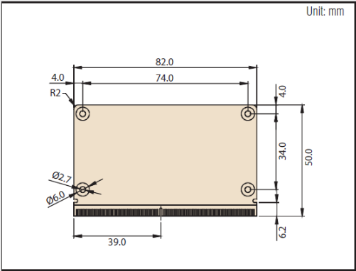
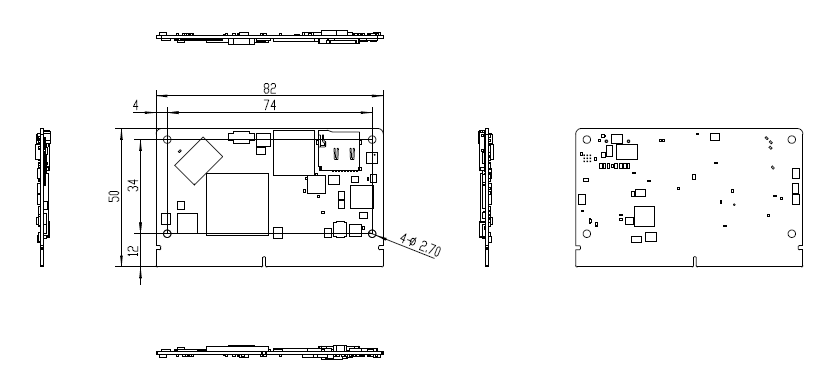
ROM-5880 机械尺寸(Mechanical Characteristics)
- Dimension: SMARC form factor size: (D x W) 82 x 50 mm/3.22 x 1.9 in
- Height on top: Under 3.0 mm
- Height on bottom: Under 2.0 mm
SOM-DB2510_A1 机械尺寸 (Mechanical Characteristics)
For more details regarding our 2D/3D models, please visit the Advantech COM support service website at: http://com.advantech.com.
Board Mechanical Diagram -Front
Board Mechanical Diagram -Side1
Board Mechanical Diagram -Side2
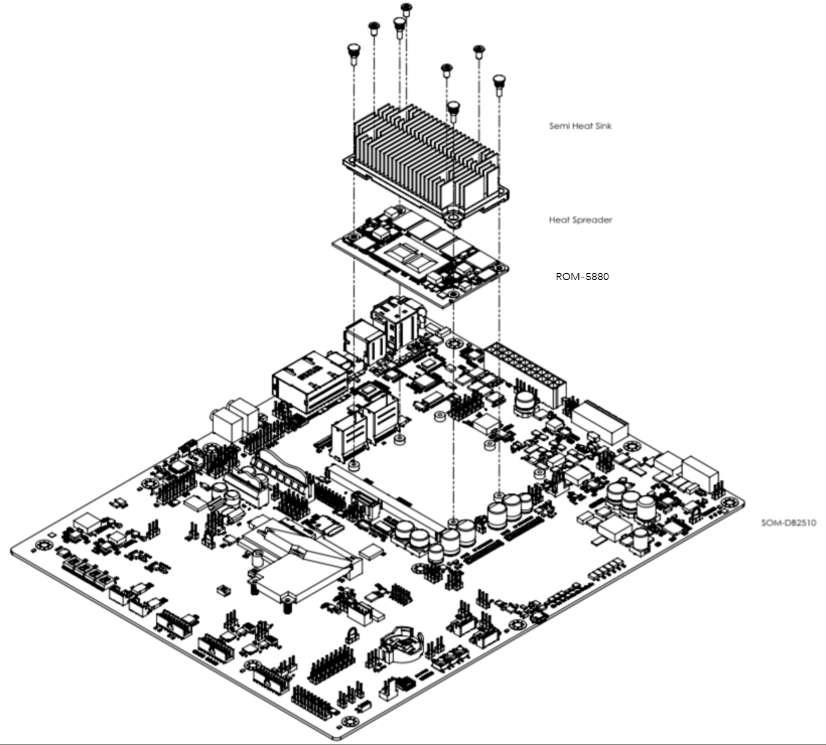
Assemblly Diagram
These figures demonstrate the order of assembly needed when attaching the thermal module and COM module to the carrier board.
快速入门 (Quick Start)
系统下载 (OS Download)
LBV=BSP,LIV=Image
| Platform | Product | Image Version | Release Date | Release Version | Release notes | Image Download | BSP Download Tag | Comment | CAN2.0 Patch |
| RK3568 | ROM-5880 | DIV130033 | 2023/08/29 | RTM | Release_Note |
Baidu Password:a887 |
RK3568_RISC_DIV130033.xml |
提取码:a887 |
Baidu Password:a887 |
- Alpha: Basic I/O function bring up by RD;
- Beta: Basic I/O function、performance and middleware verified by RD. Peripherals integrated;
- GA: Beta version by QE verification;
- RTM: Beta version by SI/Power/QE verification and pre-loaded;
Debian 燒錄方法 (Debiand Flash eMMC Method)
2. Usering bootup_sd_disk made_by SDDiskTool.
3. Upgrade with system command.
Linux基本使用方法
- Getting Start
- QT_ToolsChain
- NPU_SDK
- MAC_Address

