ROM-5880 user guide
Contents
- 1 資源特性(Features)
- 2 簡介(Introduction)
- 3 訂購資訊(Ordering Information)
- 4 規格(Specifications)
- 5 框圖(Block Diagram)
- 6 接口布局和尺寸(Layout and Sizes)
- 7 接口引脚定義 (Pin definitions)
- 8 机械尺寸 (Mechanical Characteristics)
- 9 快速入门 (Quick Start)
- 10 Android 燒錄方法 (Android Flash eMMC Method)
- 11 User Guide
- 12 通用方法(General Method)
- 13
資源特性(Features)
- Rockchip RK3568 Arm Quad Cortex-A55 up to 2.0GHz
- Onboard 2/4GB LPDDR4 memory and 16/32GB eMMC
- Support 1 x HDMI2.0 4K, 1 x signal LVDS or 1 x 2ch MIPI DSI or 1 x eDP
- Support 4K H.264/H.265 Video decoder
- 2 x USB3.0, 2 x USB2.0, 4 x UART, 14 x GPIO
- 2 x PCIe3.0, 1 x SATA, 1 x MIPI CSI, 2 x Gigabit LAN
- Support Linux & Android
簡介(Introduction)
Advantech ROM-5880 SMARC 2.1 Computer-on-Module is powered by Rockchip RK3568 SOC which includes Quad-core Arm Cortex-A55 processors and Arm Mali-G52 3D graphics
engine. It provides rich display interface: HDMI 4K@60Hz, LVDS or DSI or eDP to meet different requirement. It also features USB3.0, PCIe 3.0, SATA, Gigabit Ethernet, MIPI-CSI for
embedded applications. It is the ideal solution for POS, vending, infotainment, Medical.
ROM-5880 is paired with the Advantech SOM-DB2510 SMARC2.1 development board for faster end product peripheral integration and time-to-market. The reference schematics and
layout checklist documentations for carrier board development will be provided along with the open-sourced Linux BSP, test utilities, hardware design utilities and reference drivers.
訂購資訊(Ordering Information)
規格(Specifications)
框圖(Block Diagram)
接口布局和尺寸(Layout and Sizes)
ROM-5880 Connector Location
Connector List
Debug
| Position | Description |
| DEBUG | DEBUG Port |
Switch
| Position | Description |
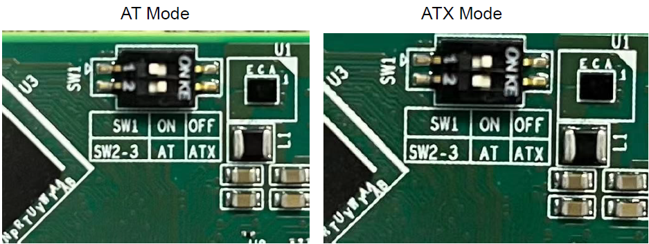
| SW1 | AT&ATX mode selection |
SW1:AT/ATX Mode Selection
| Setting | Function |
| 1 off 2 on | AT Mode(Default) |
| 1 on 2 off | ATX Mode |
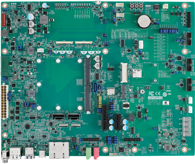
SOM-DB2510 A1 接口布局圖 Board Dimension Layout
The figures below indicate the main chips on SOM-DB2510 Development Board for SMARC 2.1.
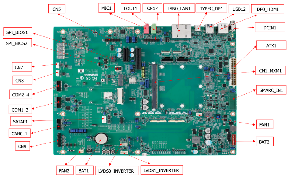
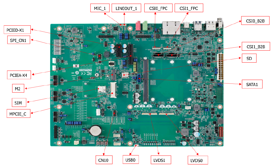
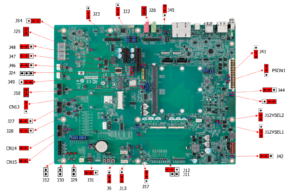
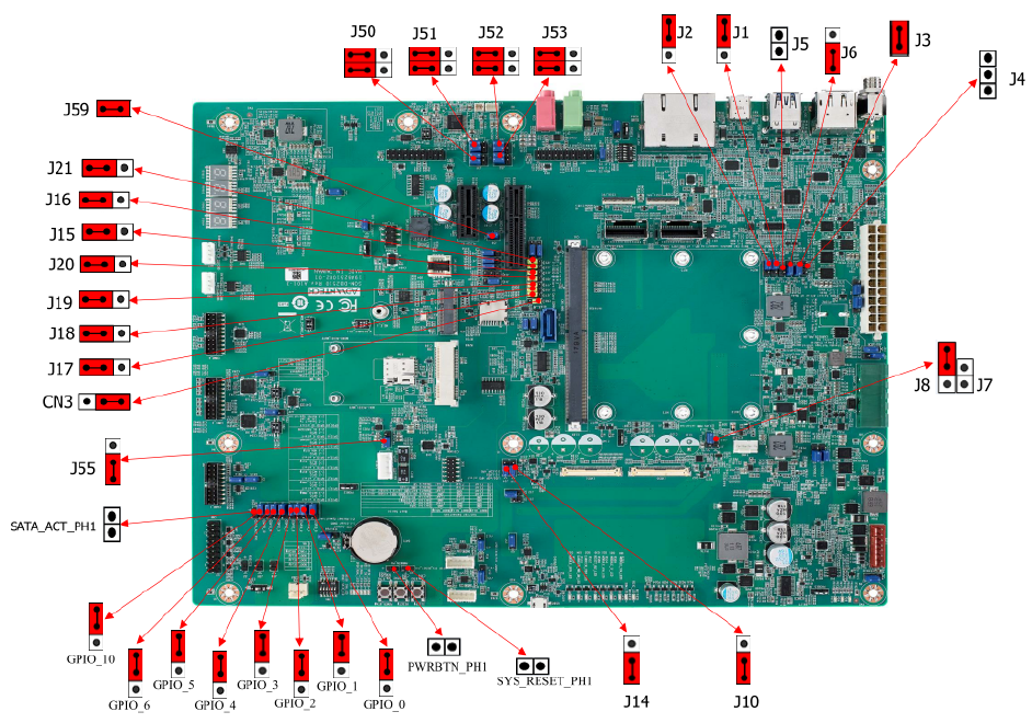
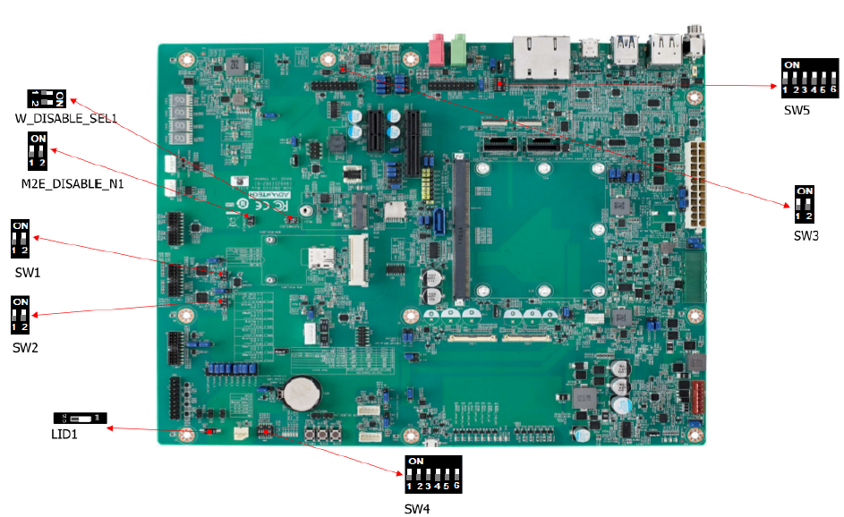
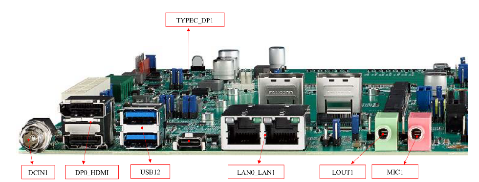
SOM-DB2510 Connectors and Jumper Settings
Connector Locations
Jumper Locations
Switch Locations
I/O Connctor Locations
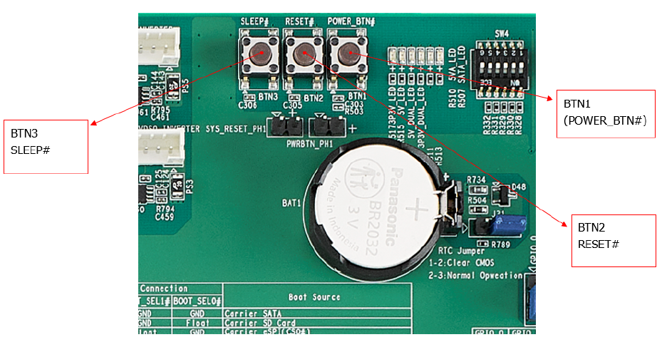
Button Locations
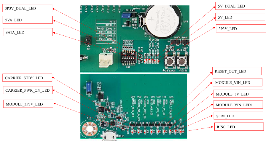
LED Locations
接口引脚定義 (Pin definitions)
Connector List
Jumper,Switch,and Button List
LED Function List
Switch Settings
SW4 Boot Select/Force Recovery/Test Switches
LID Button Enable/Disable Switches
插两张图片
机械尺寸 (Mechanical Characteristics)
For more details regarding our 2D/3D models, please visit the Advantech COM support service website at: http://com.advantech.com.
Board Mechanical Diagram -Front
Board Mechanical Diagram -Side1
Board Mechanical Diagram -Side2
Assemblly Diagram
These figures demonstrate the order of assembly needed when attaching the thermal module and COM module to the carrier board.
快速入门 (Quick Start)
系统下载 (OS Download)
Android 燒錄方法 (Android Flash eMMC Method)
User Guide


