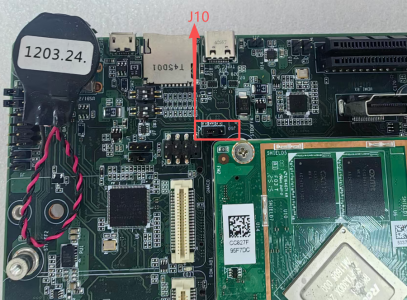
AOM-DB3500 M.2 B Key——4G/5G
From ESS-WIKI
M.2_B Key Pin define
| M.2_B M.2_B Connector Pin Definition | |||
| Pin | Signal | 1/O | Description |
| 1 | GND(Default NC) | Ground | |
| 2 | +V3.3B_M.2 | 3.3V source | |
| 3 | GND | Ground | |
| 4 | +V3.3B_M.2 | 3.3V source | |
| 5 | GND | Ground | |
| 6 | BKEY_PWR_Z_OFF | I | Active Low. A single control to turn Off WWAN solution |
| 7 | BKEY_USB_D+ | O | USB Data + Differential Signal. |
| 8 | BKEY_W_DISABLE1# | O | Aactive Low,when applied by the system it will disable radio operation on the Adapter that implement radio frequency applications. |
| 9 | BKEY_USB_D- | I/O | USB Data - Differential Signal. |
| 10 | LED1#_M2_B | O | The Adapters’ status indicators via LED devices. |
| 11 | GND | Ground | |
| 12-19 | Moudle Key | Moudle Key | |
| 20 | N/A | Not Applicable | |
| 21 | GND | Ground | |
| 22 | N/A | Not Applicable | |
| 23 | BKEY_WOWWAN#_GPIO | O | Used to wake the Platform by the WWAN device |
| 24 | N/A | Not Applicable | |
| 25 | BKEY_DPR_1.8 | O | This signal is an input directly to the WWAN Adapter from a suitable SAR sensor. |
| 26 | BKEY_W_DISABLE2# | O | Aactive Low,when applied by the system it will disable radio operation on the Adapter that implement radio frequency applications. |
| 27 | GND | Ground | |
| 28 | N/A | Not Applicable | |
| 29 | BKEY_USB3.0_RX- | I/O | USB3.0 RX - Differential signal. |
| 30 | UIM_RESET | I | UIM reset signal. |
| 31 | BKEY_USB3.0_RX+ | I/O | USB3.0 RX+ Differential signal. |
| 32 | UIM_CLK | I | UIM clock signal. |
| 33 | GND | Ground | |
| 34 | UIM_DATA | I/O | UIM data signal. |
| 35 | BKEY_USB3.0_TX- | I/O | USB3.0 TX - Differential signal. |
| 36 | UIM_VCC | I | Power source for the UIM. |
| 37 | BKEY_USB3.0_TX+ | I/O | USB3.0 TX + Differential signal. |
| 38 | N/A | Not Applicable | |
| 39 | GND | Ground | |
| 40 | N/A | Not Applicable | |
| 41 | BKEY_PERN0 | O | PCIe RX - Differential signal. |
| 42 | N/A | Not Applicable | |
| 43 | BKEY_PERP0 | O | PCIe RX + Differential signal. |
| 44 | N/A | Not Applicable | |
| 45 | GND | Ground | |
| 46 | N/A | Not Applicable | |
| 47 | BKEY_PETN0 | I | PCIe TX - Differential signal. |
| 48 | N/A | Not Applicable | |
| 49 | BKEY_PETP0 | I | PCIe TX + Differential signal. |
| 50 | BKEY_PERST# | I | Active Low.PCIe Reset is a functional reset to the card. |
| 51 | GND | Ground | |
| 52 | BKEY_CLKREQ# | I/O | Active Low.PCIe Clock Request is a reference clock request signal. |
| 53 | BKEY_PCIE_CLK- | I | PCIe Reference Clock signals (100 MHz) |
| 54 | BKEY_PEWAKE# | I/O |
Active Low. When the Adapter supports wakeup, this signal is used to request that the system return from asleep/suspend state to service a function-initiated wake event. |
| 55 | BKEY_PCIE_CLK+ | I | PCIe Reference Clock signals (100 MHz) |
| 56 | N/A | Not Applicable | |
| 57 | GND | Ground | |
| 58 | N/A | Not Applicable | |
| 59 | N/A | Not Applicable | |
| 60 | N/A | Not Applicable | |
| 61 | N/A | Not Applicable | |
| 62 | N/A | Not Applicable | |
| 63 | N/A | Not Applicable | |
| 64 | N/A | Not Applicable | |
| 65 | N/A | Not Applicable | |
| 66 | N/A | Not Applicable | |
| 67 | BKEY_RESET# | I | Active Low.The single control to Reset the WWAN solution. |
| 68 | BKEY_CLK | I | 32.768 kHz clock supply input that is provided by the Platform chipset to reduce power and cost for the Adapter. |
| 69 | GND(Default NC) | Ground | |
| 70 | +V3.3B_M.2 | 3.3 V source | |
| 71 | GND | Ground | |
| 72 | +V3.3B_M.2 | 3.3 V source | |
| 73 | GND | Ground | |
| 74 | +V3.3B_M.2 | 3.3 V source | |
| 75 | GND(Default NC) | Ground | |
J10 M.2_B Power Setting
| Pin | Function |
| J10(1-2) | M.2_B power 3.3V (Default) |
| J10(2-3) | M.2_B power 3.8V |
4G/5G
AOM-3821 supports EM05CNFD-128-SGAS and RM520NGLAA.


