Power Management
Use LPC11U14 to control power management.
Contents
Introduction
The LPC11U14 are an ARM Cortex-M0 based, low-cost 32-bit MCU family, designed for 8/16-bit microcontroller applications, offering performance, low power, simple instruction set and memory1 addressing together with reduced code size compared to existing 8/16-bit architectures.
The LPC11U14 operate at CPU frequencies of up to 50 MHz. Equipped with a highly flexible and configurable full-speed USB 2.0 device controller, the LPC11U14 bring unparalleled design flexibility and seamless integration to today's demanding connectivity solutions.
The peripheral complement of the LPC11U14 includes up to 32 kB of flash memory, up to 8 kB of SRAM data memory, one Fast-mode Plus I2C-bus interface, one RS-485/EIA-485 USART with support for synchronous mode and smart card interface, two SSP interfaces, four general purpose counter/timers, a 10-bit ADC, and up to 54 general purpose I/O pins.
Currently ROM-3420 and ROM-5420 devices support LPC11U14 MCU.
Upgrade MCU Firmware Image
You need to prepare for hardware and software.
Preparing for Hardware
- Device: ROM-3420 or ROM-5420
- MCU cable
- PC running the Microsoft® Windows® 7 or XP operating systems.
Preparing for Software
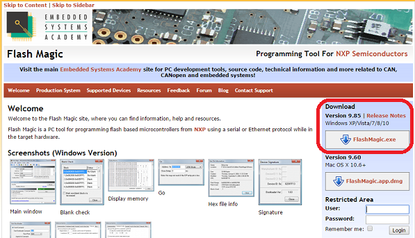
- Download flash magic tool at following URL:
http://www.flashmagictool.com/
- After downloading flash magic tool, please install this tool in the Microsoft® Windows® 7 or XP operating systems.
Upgrade MCU Firmware Image Step
Step01: Connect the device and Windows PC with MCU cable. Then power on the device. MCU light will lit.
Step02: Open Flash Magic tool in Windows PC.
Step03: When you open Flash Magic tool in Windows PC, you will see following picture.
Step04: Click to select "LPC11U14/201" device.
Step05: At "Device Manager", check COM port number in Windows PC. Then select the COM port to use or enter a COM port name.
Step06: Select or enter the "38400" baud rate to communicate with the device.
Step07: Select "None (ISP)" interface being used between Flash Magic and the device.
Step08: Enter "12" oscillator frequency on the hardware.
Step09: Select "Erase all Flash+Code Rd port". Check to erase the entire flash when the Start button is pressed.
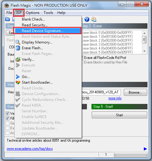
Step10: Select "ISP" item, then select "Read Device Signature..." option.
Step11: Click to select Hex file.
Step12: Click Start button to erase, program, verify, fill, generate checksums and set security bits.
Step13: After upgrading MCU firmware image, power off the device. Unplug the MCU cable. Then power on the device. MCU light will blink.
Display MCU Log Message
You need to prepare for hardware and software.
Preparing for Hardware
The user needs to prepare for hardware as following:
- Device: ROM-3420 or ROM-5420
- Debug console cable
- PC running the Microsoft® Windows® 7 or XP operating systems.
Preparing for Software
- Prepare a remote login tool. For example: PuTTy tool.
Display MCU Log Message Step
Step01: Connect the device and Windows PC with debug console cable. Then open PuTTy tool.
Step02: After entering PuTTy tool, you will see following picture.
Step03: Select "Serial" option.
Step04: At "Device Manager", check COM port number in Windows PC. Then enter "COM3" port name.
Step05: Enter the "38400" baud rate to communicate with the device.
Step06: Enter the "8" Data bits and "1" Stop bits.
Step07: Select "None" Parity and "None" Flow control. Then press "Open" button to open MCU console windows.
Step08: Power on the device and MCU light will blink.
It will display MCU log message in MCU console windows:
ULP Power sequence controller startup.
Firmware version ADV_3420 V1.05.
Change Power Sequence from 00 to 00 cause System initialize
Change Power Sequence from 00 to 1F cause Power button down
Change Power Sequence from 1F to 40 cause Watchdog Timeout
Change Power Sequence from 40 to 00 cause timeout
Step09: Press POWER button.
It will display power on sequence messages in MCU console windows:
Change Power Sequence from 00 to 1F cause Power button down
Change Power Sequence from 1F to 1E cause timeout
Change Power Sequence from 1E to 1D cause Power button up
Change Power Sequence from 1D to 1C cause timeout
Change Power Sequence from 1C to 1B cause 1V2 Power good up
Change Power Sequence from 1B to 1A cause timeout
Change Power Sequence from 1A to 19 cause 3V3 on
Change Power Sequence from 19 to 18 cause timeout
Change Power Sequence from 18 to 17 cause 5V on
Change Power Sequence from 17 to 16 cause timeout
Change Power Sequence from 16 to 15 cause 1V5 power good up
Change Power Sequence from 15 to 14 cause timeout
Change Power Sequence from 14 to 13 cause Carrier board power on
Change Power Sequence from 13 to 12 cause timeout
Change Power Sequence from 12 to 11 cause timeout
Change Power Sequence from 11 to 10 cause timeout
Step10: After the system is turned on, press POWER button 1~4 seconds.
It will display power off sequence messages in MCU console windows:
Change Power Sequence from 10 to 56 cause Power button down
Change Power Sequence from 56 to 55 cause timeout
Change Power Sequence from 55 to 54 cause Power button up
Change Power Sequence from 54 to 10 cause timeout
Change Power Sequence from 10 to 0F cause PMIC On Req down
Change Power Sequence from 0F to 0E cause timeout
Change Power Sequence from 0E to 0D cause timeout
Change Power Sequence from 0D to 0C cause timeout
Change Power Sequence from 0C to 0B cause Carrier board power off
Change Power Sequence from 0B to 0A cause timeout
Change Power Sequence from 0A to 09 cause 1V5 power good down
Change Power Sequence from 09 to 08 cause timeout
Change Power Sequence from 08 to 07 cause 5V off
Change Power Sequence from 07 to 06 cause timeout
Change Power Sequence from 06 to 05 cause 3V3 off
Change Power Sequence from 05 to 04 cause timeout
Change Power Sequence from 04 to 03 cause 1V2 Power good down
Change Power Sequence from 03 to 02 cause timeout
Change Power Sequence from 02 to 01 cause timeout
Change Power Sequence from 01 to 00 cause Power button up
Step11: After the system is turned on, press SLEEP button.
It will display sleep sequence messages in MCU console windows:
Change Power Sequence from 10 to 53 cause Sleep button down
Change Power Sequence from 53 to 52 cause timeout
Change Power Sequence from 52 to 51 cause Sleep button up
Change Power Sequence from 51 to 50 cause timeout
Change Power Sequence from 50 to 10 cause timeout
Change Power Sequence from 10 to 2F cause Standby on
Change Power Sequence from 2F to 23 cause timeout
Change Power Sequence from 23 to 22 cause timeout
Change Power Sequence from 22 to 21 cause 5V off
Change Power Sequence from 21 to 20 cause timeout
Step12: After the system enters sleep mode, press WAKE button.
It will display wake up messages in MCU console windows:
Change Power Sequence from 20 to 3F cause WAKE button down
Change Power Sequence from 3F to 37 cause timeout
Change Power Sequence from 37 to 36 cause WAKE button up
Change Power Sequence from 36 to 35 cause timeout
Change Power Sequence from 35 to 34 cause timeout
Change Power Sequence from 34 to 33 cause timeout
Change Power Sequence from 33 to 32 cause 5V on
Change Power Sequence from 32 to 31 cause timeout
Change Power Sequence from 31 to 10 cause Standby off
Step13: After the system is turned on, press RESET button.
It will display rest sequence messages in MCU console windows:
Change Power Sequence from 10 to 12 cause Reset detected
Change Power Sequence from 12 to 11 cause timeout
Change Power Sequence from 11 to 10 cause timeout


